
Definition#
Look up table is a memory. Instead of recomputing a circuit or a logic function every time, we compute and store in LUTs. Then depending on the input, FPGA looks up from the table and output that result.
How it Works#
Look up tables operates like a memory.
Let’s say you want you implement the Boolean logic ($A$ AND $B$) OR ($\bar{A}$ AND $\bar{B}$).
One way we can do this is to make the digital circuit. This will however require 3 gates. And most importantly a lot of space with no flexibility. (Once you implement this, you can’t really erase it and reuse for another logic function)
Another way to do this, is you get the expression and fill out its truth table.
$$F = (A \space AND \space B) \space OR \space (\bar{A} \space AND \space \bar{B})$$
| A | B | F |
|---|---|---|
| 0 | 0 | 1 |
| 0 | 1 | 0 |
| 1 | 0 | 0 |
| 1 | 1 | 1 |
Then you store the outputs in the table (F) and store them in a memory, a component we call LUTs. These bits are stored in sram cells in the LUT.
Physical Implementation#
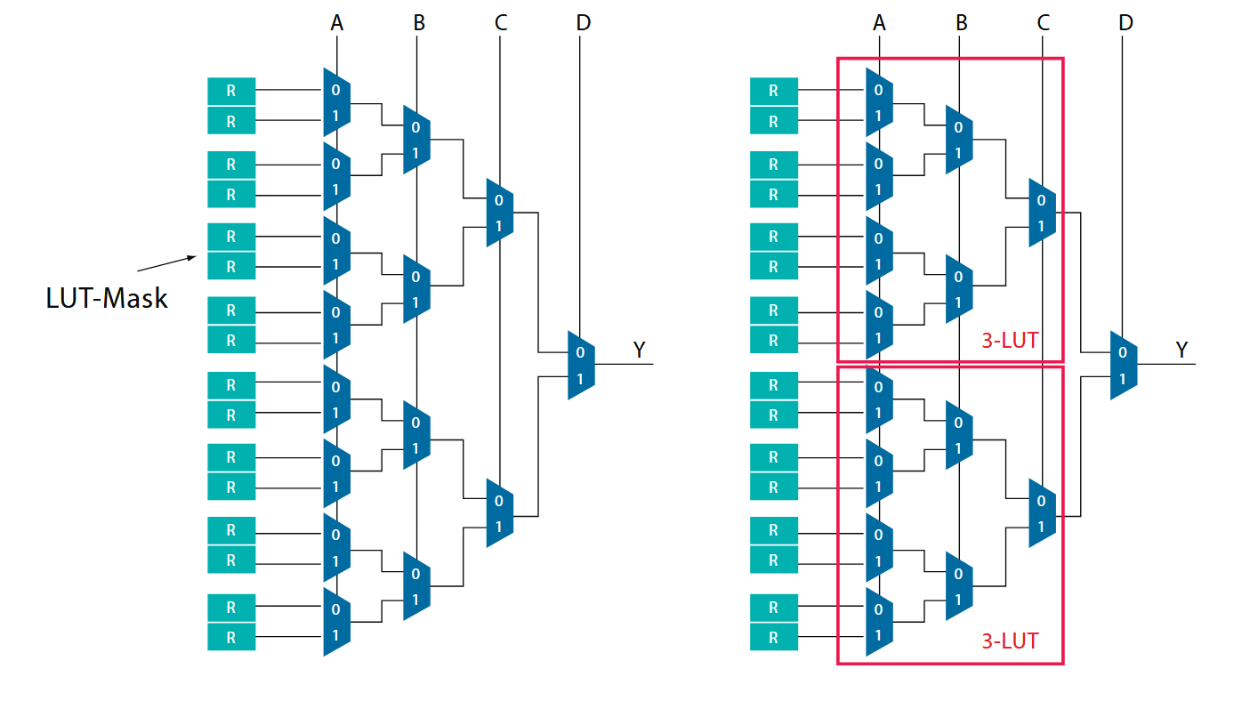
LUTs are built out of SRAM bits to hold the configuration memory (CRAM) LUT-mask and a set of multiplexers to select the bit from CRAM that is going to drive the ouput.
A k-input LUTs holds $2^k$ configuration bits. For example, a 4-input LUT can realize any Boolean function of four variables by treating its inputs as the address lines of a 16-entry table whose contents you program.
To implement a k-input LUT (k-LUT) - we need $2^k$ SRAM bits and a $2^k$ : 1 multiplexer.
Retrieving Results#
During runtime, when you perform the “Look up” function, your variables/inputs work as the address of the entry you want to look up. We use multiplexers for this where the inputs now are your select lines for the multiplexers.