
![]()
At the heart of an SRAM cell lies a bistable flip-flop, which is a circuit capable of holding one of two stable states: logic ‘0’ or logic ‘1’. This flip-flop is typically constructed using two cross-coupled inverters
How Cross-Coupled Inverters Form a Flip-Flop#
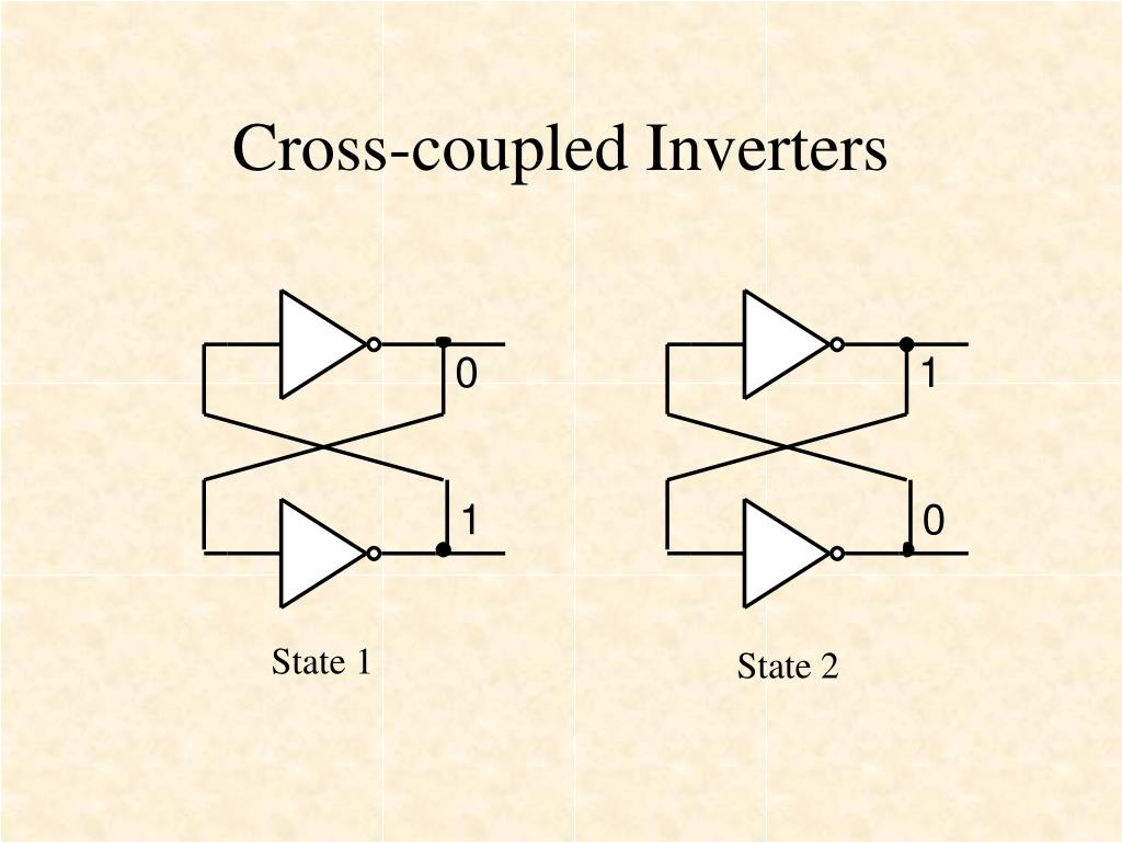
A flip-flop is a circuit with two stable states, capable of storing one bit of information. In SRAM, this is achieved by connecting two inverters in a loop:
Inverter A: Takes input from the output of Inverter B.
Inverter B: Takes input from the output of Inverter A.
This cross-coupling creates a feedback loop where the output of each inverter reinforces the input of the other. As a result, the circuit stabilizes in one of two states:
State 1: Output of Inverter A is ‘1’; Output of Inverter B is ‘0’.
State 2: Output of Inverter A is ‘0’; Output of Inverter B is ‘1’.
These two stable states correspond to the stored bit being ‘1’ or ‘0’, respectively.
Here is a graph to illustrate how it stays stable.
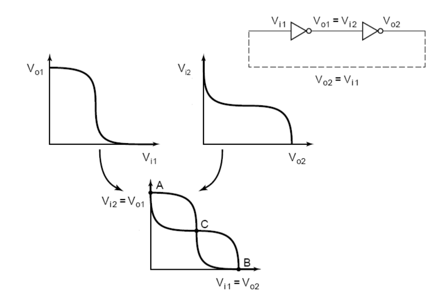
(From https://engineering.purdue.edu/~vlsi/courses/ee695kr/s2008/Lecture4.pdf)
How Transistors Form an Inverter#
A CMOS (Complementary Metal-Oxide-Semiconductor) inverter consists of two types of transistors:
PMOS (P-type MOSFET): Conducts when the gate voltage is low.
NMOS (N-type MOSFET): Conducts when the gate voltage is high.
These transistors are connected in a specific configuration:
PMOS Transistor:
Source connected to the positive supply voltage (VDD).
Drain connected to the output node.
Gate connected to the input signal.
NMOS Transistor:
Source connected to ground (GND).
Drain connected to the output node.
Gate connected to the input signal.
The gates of both transistors are tied together and serve as the input, while their drains are connected together to form the output.
Operation:
Input Low (0V):
PMOS is ON (conducting), NMOS is OFF (non-conducting).
Output is pulled up to VDD (logic high).
Input High (VDD):
PMOS is OFF (non-conducting), NMOS is ON (conducting).
Output is pulled down to GND (logic low).
This configuration ensures that the output is always the logical inverse of the input, hence functioning as an inverter.
References#
https://engineering.purdue.edu/~vlsi/courses/ee695kr/s2008/Lecture4.pdf